Nvidia is not the only company that has created specialized compute units that are good at the matrix math and tensor processing that underpins AI training and that can be repurposed to run AI inference. Intel has acquired two such companies – Nervana Systems and quickly right after that Habana Labs, and it is the latter that has been productized by Intel and set on the heels of Nvidia’s GPU accelerators.
Intel is in good company chasing what the company thinks will be a $50 billion AI compute opportunity (for both training and inference) in the next five years, growing at a 25 percent compound annual growth rate between now and 2027 to reach that level. Given the sizeable matrix and vector math coming int eh “Ponte Vecchio” Xe HPC GPU accelerator, and the very likely sufficient inference capacity in the AMX matrix math units in the impending “Sapphire Rapids” Xeon SP CPUs, it is reasonable to wonder how many Gaudi training and Goya inference chips that Intel expects to sell.
We understood that Intel was after intellectual property and people when it did the $350 million Nervana Systems deal in August 2016 and the $2 billion Habana Labs acquisition in December 2019, of course, because that is how this IT war is played, but we always wondered if these devices, as well as very elegant and interesting designs from competitors GraphCore, Cerebras, SambaNova Systems, and Groq, would ever be deployed in something resembling the mainstream. The private equity investors have been eager to get onto this AI chip gravy train and have invested heavily, with the four companies mentioned above raising a combined $2.87 billion to date.
The jury is still out, all of these products are just getting rolling, and that is why Intel is hedged its bets with the Nervana and then Habana, just like it freaked out about FPGAs in the datacenter (thanks mostly to Microsoft Azure) and shelled out $16.7 billion to acquire Altera back in June 2015. Between 2015 and 2020, when Intel reined supreme in datacenter compute, it was trying to eliminate every possible threat to its hegemony with Xeon CPU compute, and it could afford to buy some of its competition .
Now, since it has remembered that it needs to be a foundry once again, it can no longer make such expensive maneuver offenses that are really as much about defense as they are offense. And now it is time to try to make some of that money back that it paid for Nervana and Habana. It is unclear if Intel can ever get all of its money back, even at the $2.35 billion investment that it made, but as we say, maybe that was not the point. Maybe the point was to have a counter-argument to GraphCore, Cerebras, SambaNova Systems, and Groq as Intel added AI features to its Xeon SP CPUs and got its discrete GPUs out the door this year. (Wave Computing, which raised $203.3 million to develop its AI chips, went bankrupt in April 2020 and emerged as a supplier of MIPS chip technology a year later, so we are not counting it among the AI chip contenders anymore.)
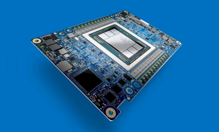
At the Intel Vision 2022 conference being held this week, the Gaudi2 AI training chip was the big new compute engine that the chip maker trotted out, and incidentally, it is not a chip that Intel actually makes but is rather, like its predecessor, the Gaudi1, etched by rival foundry Taiwan Semiconductor Manufacturing Co.

Like Nervana Systems, Habana Labs is deadly serious about creating a set of chips that deliver the best bang for the buck and the best performance for AI workloads. The Habana Goya HL-1000 inference chip was announced in early 2019, and the Gaudi1 AI training chip, also known as the HL-2000, debuted later that summer. The Gaudi1 architecture has a general matrix multiply (GEMM) front end that is back-ended by ten Tensor Processor Cores, or TPCs, and the chip only exposed eight of them to users to help increase the yield of the package. (Apparently, the extra two tensor cores were exposed at some point after Intel acquired Habana Labs.)
The Gaudi1 used the second generation of the TPCs while the Goya HL-1000 AI inference chip used a less beefy and less sophisticated original TPC design. The TPCs in the Gadui1 chip are directly addressable using the C programming language and have tensor addressing as well as support for BF16 and FP32 floating point and INT8, INT16, and INT32 integer formats. The TPC instruction set has circuits to accelerate Sigmoid, GeLU, Tanh, and other special functions. The Gaudi1 was implemented in TSMC’s 16 nanometer processes, and had 24 MB of on-chip SRAM, four banks of HBM2 memory weighing in at 32 GB of capacity and 1 TB/sec of bandwidth. The Gaudi1 plugged into a PCI-Express 4.0 x16 slot and consumed 350 watts of juice and converted almost all of it to heat, as chips do. (A small amount of energy is used to manipulate and store information.)

Intel has yet to reveal the deep dive on the Gaudi2 architecture, but here is what we know.
With the Gaudi2, Intel is moving to TSMC’s 7 nanometer processes, and with that shrink it is able to increase the number of TPCs on the chip from 10 to 24, and added support for the new 8-bit FP8 data format that Nvidia has also added to its “Hopper” GH100 GPU compute engines, which launched in March and which ship in the third quarter. With the FP8 format, it will now be possible to have low resolution inference data and high resolution training data in the same format, and not have to convert models between floating point and integer when moving from training to inference. This is a real boon for AI, although lower precision integer formats may remain in matrix and vector compute engines for many years to come to support legacy code and other kinds of applications. The Gaudi2 chip has 48 MB of SRAM – you would have expected 2.4X not 2X more SRAM, or 57.6 MB, if it had scaled linearly with the TPC count.
Hanging off the Gaudi2 chip are banks of HBM2e memory, which deliver 2.45 TB/sec of bandwidth, a factor of 2.45X increase over the Gaudi1 chip. The number of banks of HBM2e memory was not revealed, but six banks of 16 GB HBM2e does the trick for the Gaudi2 compared to four banks of 8 GB HBM2 for the Gaudi1. That increase in two HBM2e memory controllers alone would increase bandwidth by 1.33X, and the remaining increase in bandwidth comes from cranking the memory speed up.
The Gaudi1 chip had ten 100 Gb/sec Ethernet ports that supported the RoCE direct memory access protocol – one for each TPC, as it turns out, but we didn’t know that at the time because only eight were shown. But the Gaudi2 has 24 Ethernet ports running at 100 Gb/sec, again one for each TPC. It weighs in at 650 watts. We presume this device plugs into a PCI-Express 5.0 slot, but Intel has not confirmed this.
Assuming no major architectural changes and a modest bump in clock speed engendered by the process shrink from 16 nanometers down to 7 nanometers, we expect that the Gaudi2 chip would deliver about 2.5X the performance of the Gaudi2. (Also assuming the same level of precision for processing in any given application.) But Intel has not actually said if there are any architectural changes (other than it has added some media processing functions) and how the clock speeds have changed, so we have to infer that.
Which we did by looking at this chart on ResNet-50 machine vision training operations, which pits the Gaudi1 and Gaudi2 against the past two generations of Nvidia GPU accelerators:

Based on this ResNet-50 comparison, the Gaudi2 is delivering 3.2X the performance of the Gaudi1, but it is hard to reckon how much of the performance is due to what increased capacity across the chip. This particular test is running the TensorFlow framework to do image recognition training, and the data shown is for the number of images processed per second.
The one thing that is not shown, and which is important, is how the Gaudi2 accelerator will stack up to the Hopper GPU, but Nvidia has not disclosed performance results on any specific test as yet. But with the HBM3 memory in the H100 running 1.5X faster than the HBM2e memory used in the A100 accelerator and FP16, TF32, and FP64 delivering 3X the performance on the new Tensor Cores, it is reasonable to expect that the H100 will deliver somewhere between 1.5X and 3X the performance on ResNet-50 vision training workloads, and therefore the H100 will deliver somewhere between 4,395 and 8,790 images per second of performance on the ResNet-50 test. Our guess is it will be closer to the latter than the former, and a considerable margin over and above what Intel can deliver with Gaudi2.
Image recognition and video processing are relatively easy compared to natural language processing using the BERT model. Here is how Gaudi2 stacked up against the Nvidia V100 and A100, and notice the Gaudi1 is missing:

The BERT model is also running atop the TensorFlow framework, and this data shows the number of sequences per second of throughput in two different phases of training. In a prebriefing, Eitan Medina, chief business officer at the Habana Labs division, said that the Gaudi2 delivered just under 2X the performance of the A100. But the H100, with its own FP8 format and its Transformer Engine that dynamically shifts the precision of the data and processing for different parts of the AI training workflow, could do substantially better. We don’t know by how much, but we strongly suspect that Nvidia can at least close the gap with Gaudi2 and very likely surpass it.
Just to make things interesting, Intel fired up DL1 Gaudi1 instances on Amazon Web Services and then the p4d and p3 instances based on the A100 and V100 GPUs, respectively, and did some price/performance analysis to calculate the cost per image recognized in the ResNet -50 benchmark. Take a gainer at this:

What this chart means is that the Gaudi1 offers slightly better performance than the V100 – 27.3 percent using Intel’s performance data in the chart above for ResNet-50 – and about 60 percent better bang for the buck, which means the DL1 instance costs considerably less than the p3 instance using the V100. With the move to the A100-based p4d instance, which has 40 GB of HBM2e memory, the Nvidia device has 58.6 percent more throughput on ResNet-50 than the Gaudi1, but the Gaudi1 has 46 percent lower cost per image processed. Which means that A100 instance is quite a bit more expensive indeed. And if our guess about Hopper GPU accelerator pricing is correct, and Nvidia charges roughly 2X as much for roughly 3X as much performance, and Intel will have to keep the price of the Gaudi2 chips sold to AWS at a place where AWS can still show better price/performance than the H100 instances running AI training.
And just where is Trainium in all of this? hmmm. . . .
Anyway, Intel has over 1,000 of its Gaudi2 in its labs running so it can tune up the SynapseAI software stack, which includes the PyTorch and TensorFlow frameworks running atop Habana’s graph compiler, kernel library and communications libraries. The Gaudi2 chip is shipping now.
In addition to the Gaudi2 chip, Intel is also previewing its Greco follow-on Goya inference engine, which is also making the jump to 7 nanometer to 16 nanometer processes at TSMC.

The Greco inference card has 16 GB of LPDDR5 main memory, which delivers 204 GB/sec of memory bandwidth compared to the 40 GB/sec of with a 16 GB chunk of DDR4 memory with the prior Goya inference engine. This Greco variant of the Habana architecture supports INT4, BF16, and FP16 formats and consumes 75 watts, down substantially from the 200 watts of the HL-1000 device announced in early 2019. And as the image above shows, it is being compressed down to a more compact half height, half length PCI-Express card. No word on performance or pricing for this one as yet.